简体中文
简体中文
 English
 عربى
عربى
Content
For an engineer specifying interconnects, a procurement manager sourcing bearing cages, or a product designer optimizing heat dissipation, copper stamping parts often represent a convergence of performance and manufacturability that few other component types can match. The challenge is not whether copper can be stamped, but how to select the right alloy, define tolerances that balance cost and function, and ask suppliers the right questions before the first tool is cut.
What Are Copper Stamping Parts?
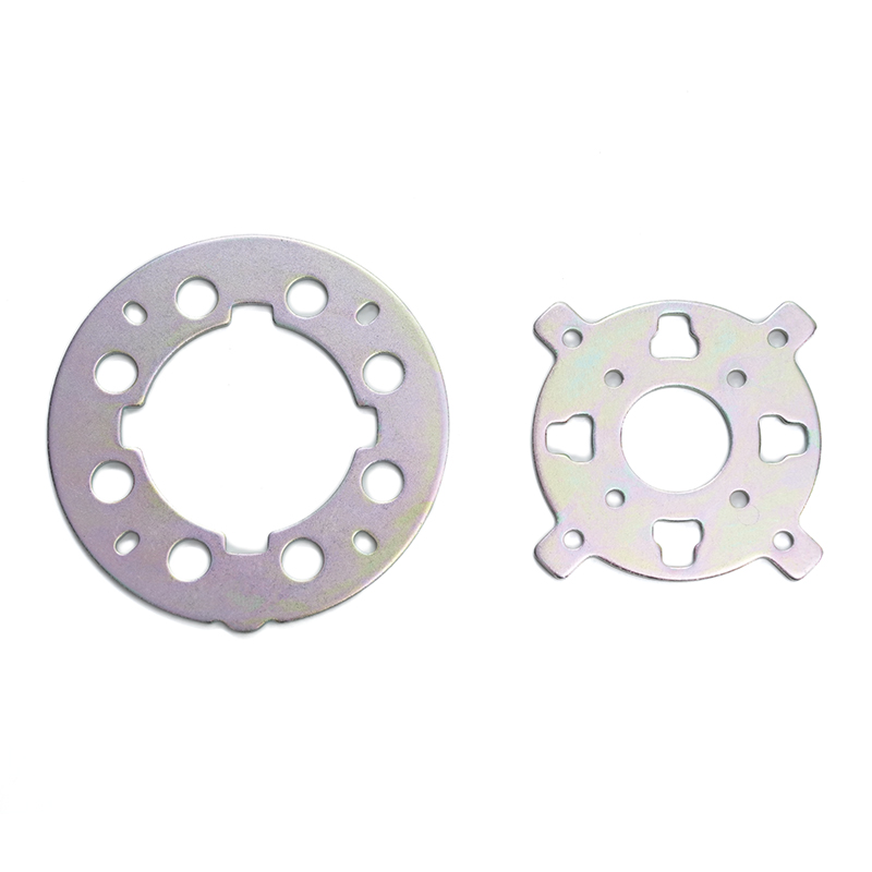
Copper stamping parts are precision metal components produced by feeding copper or copper alloy strip through a progressive or compound stamping die under high tonnage. The strip is blanked, pierced, bent, drawn, and coined in a sequence of stations, often at speeds exceeding 200 strokes per minute. The result is a net-shape part that meets tight dimensional requirements with minimal secondary processing—critical in high-volume electrical, automotive, and industrial applications.
Process Overview
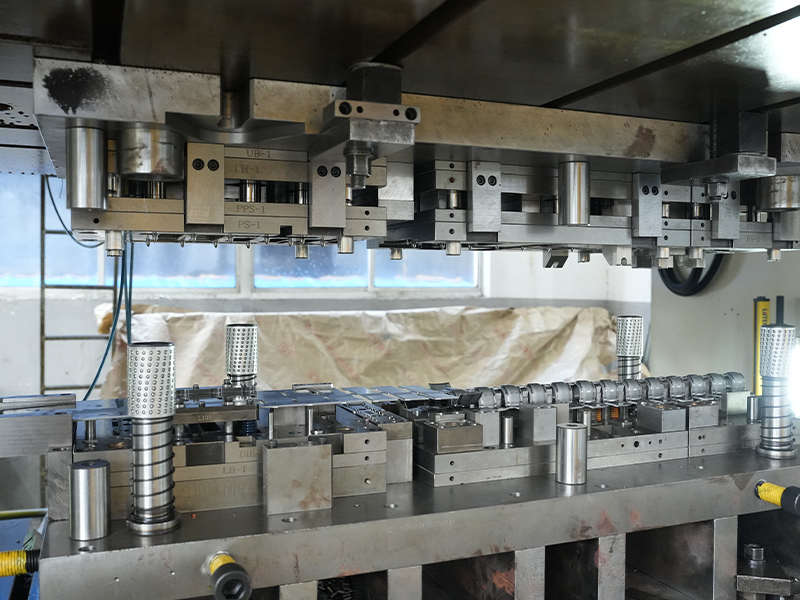
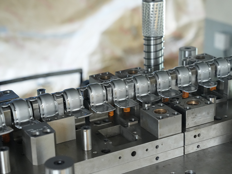
The manufacturing sequence begins with copper strip, typically between 0.05 mm and 3.0 mm thick, fed from a coil into a press. A progressive die performs multiple operations in a single stroke. The continuous nature of the process enables consistent part-to-part repeatability and supports annual volumes from 100,000 to tens of millions of pieces. Key steps include piloting for precise alignment, blanking the outer profile, forming features such as radii or embossments, and separating the finished part from the carrier. Advanced tooling integrates in-die sensing and vision systems to catch deviations in real time.
Why Choose Copper?
Copper’s electrical conductivity (up to 100% IACS for pure grades) makes it the material of choice for current-carrying components. Its thermal conductivity, approximately 20 times that of stainless steel, pulls heat away from sensitive junctions in power modules and LED assemblies. In addition, copper offers natural corrosion resistance without the need for protective plating in many indoor environments, and its high ductility permits forming into complex shapes that would crack less malleable materials. Compared to aluminum, copper stamping parts eliminate the risk of galvanic corrosion when mated with copper conductors and reduce termination failure modes over the product lifecycle.
Choosing the Right Copper Alloy
Selecting an alloy is the single most consequential decision in the specification process. Electrical, mechanical, thermal, and economic factors must be weighed against the intended operating environment. The three most commonly stamped copper families—pure copper, brass, and phosphor bronze—each present a distinct trade-off profile.
Pure Copper, Brass, Phosphor Bronze
| Alloy | Conductivity (%IACS) | Typical UTS (MPa) | Ductility | Primary Advantage |
|---|---|---|---|---|
| C11000 (ETP Copper) | 100 | 220–310 | Excellent | Highest electrical/thermal conductivity |
| C26000 (Cartridge Brass) | 28 | 310–580 | Good | Machinability and cost balance |
| C51000 (Phosphor Bronze) | 15 | 470–690 | Moderate | Fatigue resistance and spring properties |
Pure copper (C11000) is unmatched for bus bars, power distribution contacts, and heat sinks where minimal voltage drop or maximum thermal transfer is required. However, its low yield strength limits its use in spring-loaded contacts. Brass (C26000) offers a favorable balance of strength, corrosion resistance, and lower raw material cost, making it ideal for connectors, terminals, and decorative industrial fittings. Phosphor bronze (C51000) provides the best combination of spring properties and fatigue life, relied upon in billions of electrical contact springs and EMI shielding fingers every year. This alloy’s ability to maintain contact force over thousands of mating cycles makes it indispensable in connectors and relay sockets.
Material Selection Factors
Beyond conductivity and strength, the selection matrix should include formability (R/t ratio limitations), stress relaxation resistance at elevated temperature, and compatibility with subsequent plating or welding processes. For a CPU heat sink fin, thermal diffusivity and ease of soldering dominate; for a bearing cage, fatigue strength under cyclic loading and oil compatibility take priority. Starting with the dominant failure mode in the application—electrical overheating, mechanical fracture, or corrosion—narrows the alloy field quickly and prevents over-specification that drives up material costs.
Design and Manufacturing Considerations
Even an optimal alloy choice will fail to deliver yield and quality if the part geometry ignores the fundamentals of sheet metal deformation. Early collaboration between the design engineer and the stamping supplier can shorten tooling lead time and avoid costly field failures.
Bend Radius and Springback
A minimum inside bend radius of one material thickness is a safe starting point for most copper alloys, but tighter radii are feasible in annealed materials with the grain direction oriented favorably. Springback—the elastic recovery that causes the bent angle to open after the punch retracts—must be compensated in the tool geometry. Copper alloys typically exhibit less springback than stainless steel, yet phosphor bronze can require overbend angles of 2° to 6° depending on temper. Prediction of springback using finite element simulation reduces tryout iterations and ensures dimensional stability across the coil lot.
Tolerances and Precision Control
Progressive stamping can routinely hold dimensional tolerances of ±0.05 mm on critical features, with tighter limits achievable through in-die coining or shaving stations. Hole size, pitch distance, and flatness requirements should be reviewed against industry standards such as ISO 2768. For thin-walled copper bearing cages, for instance, maintaining consistent wall thickness and concentricity within 10 µm determines the cage’s dynamic balance and noise level in precision motor applications. A supplier with in-house tooling design and CNC grinding capabilities is better positioned to hold micro-tolerances over millions of hits.
Surface Finishing and Post-Treatment
Many copper stampings are used as-formed, relying on the native corrosion resistance. When additional protection or solderability is required, electroplated tin, silver, or nickel finishes are applied using selective or overall plating processes. Passivation treatments and anti-tarnish coatings are common for brass components destined for visible or harsh environments. The stamping supplier should validate plating adhesion through thermal shock testing and measure coating thickness in micro-sections.
Typical Applications of Copper Stamping Parts
The versatility of stamped copper components is reflected in their presence across industries, from nanometer-scale chip interconnects to heavy-duty industrial switchgear. The following examples represent high-value applications where copper’s properties directly enable product performance.
Electrical and Electronic Components
Over 60% of copper consumption in stamped form ends up in electrical distribution and electronic interconnection. Terminal blocks, fuse clips, ground straps, and EMI/RFI shields are produced in the billions annually. Phosphor bronze stamped contacts are the backbone of modular connectors and smart card readers, where consistent insertion force and long-term reliability are non-negotiable.
Automotive and Industrial Bearings
Copper alloy stampings play a critical but often unseen role in rotating equipment. Thin-walled copper bearing cages retain rolling elements in high-speed electric motor bearings, combining light weight with excellent lubricant compatibility. Brass bearing dust caps and seal retainers protect against contamination while maintaining precise axial location. These components must withstand centrifugal forces, thermal cycling from -40 °C to 150 °C, and millions of rotational cycles without deformation.
Thermal Management Solutions
From CPU heat sink fins to power semiconductor baseplates, stamped copper parts provide the thermal path necessary to keep junction temperatures within safe operating limits. Skived or stamped copper fin arrays offer high surface area and low air-side pressure drop, critical in server cooling. The ability to stamp intricate fin geometries and then solder or braze them onto heat pipes demonstrates the range of complementary processes a competent stamping supplier can coordinate.
Sourcing Copper Stamping Parts: A Buyer’s Checklist
A well-prepared RFQ package accelerates quoting accuracy and reveals a supplier’s technical depth before tooling investments are made. The following sections outline what information to compile and how to assess manufacturing competence.
What to Prepare Before Requesting a Quote
- Detailed 2D drawing and 3D CAD model: Include all critical dimensions, tolerances, and datum references.
- Material specification: Alloy grade, temper (e.g., H02, H04), and any preferred supplier certifications.
- Annual volume and delivery cadence: Quantify whether the part is a steady-run item or spiky project-based demand.
- Surface finish requirement: Specify if bare copper is acceptable or if plating, passivation, or cleaning residues limits apply.
- Application environment: Operating temperature range, exposure to chemicals, and mating part materials reveal latent risks that influence material and plating choices.
Quality Verification and Certifications
A competent copper stamping supplier will demonstrate statistical process control through process capability indices (Cpk ≥ 1.33 for critical characteristics) and maintain an ISO 9001-certified quality management system. For automotive-grade safety components, IATF 16949 certification adds an extra layer of defect prevention and traceability. Incoming material certificates should show compliance with ASTM B152 or equivalent, and lot traceability back to the mill is standard expectation. First-article inspection reports containing full dimensional layout, conductivity measurements, and micrographic cross-section of stamped edges provide objective evidence of process maturity.
Evaluating Supplier Capabilities
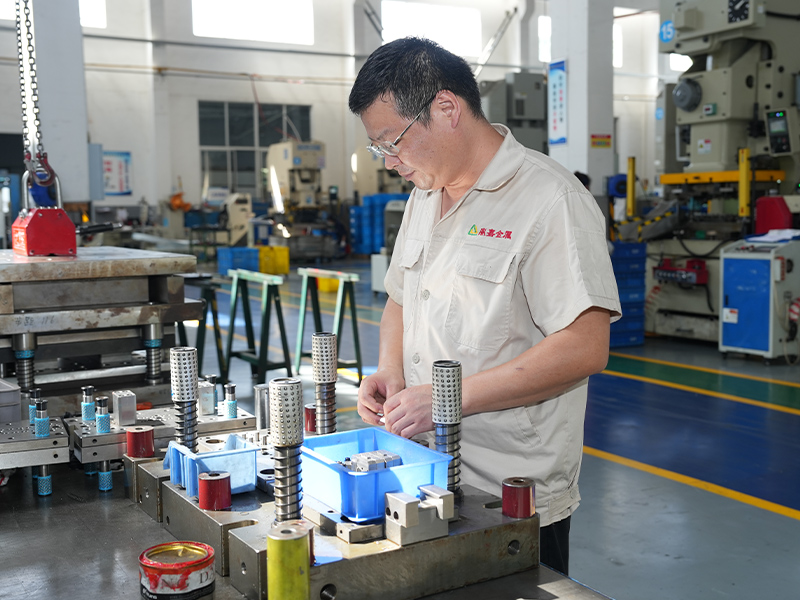
Beyond price per piece, assess the breadth of in-house tooling design and manufacturing, press tonnage range (typically 25 to 400 tons for copper stamping), and secondary operations such as tapping, riveting, or automated optical inspection. A supplier that designs its own progressive dies and maintains a tool history database can react faster to design changes and proactively schedule tool maintenance. Look for documented experience in producing thin-walled copper bearing cages, intricate heat sink fins, or continuous phosphor bronze contact strips—these applications demand deep material knowledge and process control that generic stamping houses lack.
Precision copper stamping sits at the intersection of materials science, tool engineering, and volume manufacturing economics. By anchoring the specification to the dominant functional requirement and asking suppliers detailed process questions early, engineering and procurement teams can secure components that meet performance targets without hidden cost premiums. The best copper stamping outcomes come from design-manufacturing partnerships where the supplier’s material and tooling expertise is engaged from concept stage onward.